


We describe our research activity on microelectromechanical (MEMS) and nanoelectromechanical (NEMS) devices made with thin films of oxides deposited by the pulsed laser ablation technique.
To view individual sections:
MICROELECTROMECHANICAL SYSTEMS
MEMS - an acronym for MicroElectroMechanical Systems - or microsystems are essentially miniaturized devices that include electronic circuits and moving elements of sub-millimeter size, such as mirrors, levers or membranes that add mechanical, electrical and optical functionalities to the device. The term "MEMS" also indicates the set of processes necessary for the realization of these systems. MEMS technology developed from integrated circuit fabrication techniques (microprocessors) and later specialized, becoming a field in its own right. MEMS often consist of three-dimensional silicon structures integrated with ultra-thin layers (called "films") of metal elements or materials with specific functionality.
A popular MEMS device is the accelerometer, a sensor used in every smartphone. The accelerometer comprises a micrometer-sized mass of silicon held suspended by spring-acting joints, and therefore free to move. This mass is the mechanical part of the accelerometer. When subjected to acceleration, the mass moves relative to the rest of the microchip in analogy with what happens to our body when we accelerate in a car. The change in position with respect to the rest of the microchip can be measured electrically via an electronic circuit integrated into the accelerometer itself. In commercial MEMS devices, the moving elements – and the circuits necessary for their measurement – are often parts of the same electronic component, sometimes made by coupling the two parts after their manufacture.
MEMS are widely used in the electronics industry and are found in most objects in our daily lives. For example, our smartphone often includes an accelerometer, an electronic compass, a gyroscope, a radio frequency filter, a microphone, an autofocus system; all these devices are based on MEMS technology [Ref.1].
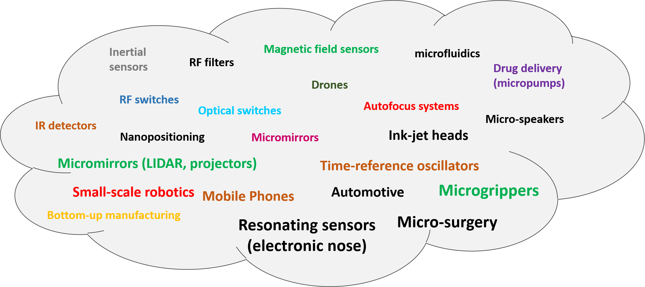
Figura 1- Applications of MEMS
Nano-electro-mechanical systems (NEMS) are smaller than MEMS and operate at the nanoscale (nanodevices are objects with at least one size below 100 nanometers); NEMS are still mainly made in research laboratories and are used to make high-sensitivity sensors with various applications such as detecting molecules in the air, measuring magnetic fields or light radiation, or even in quantum physics experiments.
The M/NEMS world is very fascinating and multidisciplinary, as their development requires knowledge in the fields of electronics, mechanics, optics and materials science.
OXIDES
Oxides are part of our daily lives. Oxygen is the most abundant element on Earth and is very reactive, consequently many minerals present in the subsoil are oxides. Oxides have been essential to the development of technology over the centuries. For example, magnetite (Fe3O4) was used in ancient history for the manufacture of the first compasses due to its intrinsic magnetism (magnetite is precisely a ferrimagnet). Silicon oxide is used in its amorphous phase as an insulating material (dielectric) in current transistor technology, while in one of its crystalline phases, called quartz, it is used as a mechanical oscillator for clocks and timing components. Quartz is in fact known for an important property: piezoelectricity, or the ability to generate a voltage when deformed by external pressure. In addition, quartz deforms when subjected to an external voltage signal (reverse piezoelectric effect). Piezoelectric oxides as well as Pb(Zr,Ti)O3, called PZT, are now widely used in electronic devices and micromechanical components. One of the most fascinating properties of oxides was discovered in 1986, when it was observed that some copper oxides became superconducting at a relatively high temperature compared to traditional metal-based superconductors such as niobium. The most well-known critical high temperature superconductor today is YBa2Cu3O7 –x , or YBCO, a complex oxide that is used to make Josephson junctions and SQUID-type magnetometers that operate above the temperature of 77 K, the boiling point of liquid nitrogen. Scientific research on YBCO has stimulated the scientific community to study the properties of many other oxide compounds defined as "complex" and to create artificial structures not present in nature such as superlattices and oxide heterostructures, i.e. artificial structures made by depositing several layers of different oxides on top of each other, sometimes alternating the compounds themselves in periodic sequences.
Some oxides change their properties as the temperature changes. For example, they can abruptly change their volume, their magnetic, electrical, and optical properties. This aspect is of particular interest for the development of new types of mechanical sensors and actuators (actuators are devices that transform an energy source into a controlled force or mechanical movement) based on local temperature variations. One of our research projects concerns the development of micromechanical actuators based on vanadium dioxide, VO2, the subject of a past collaborative project between the National Research Council, the University of Genoa and the University of Osaka [Ref. 2].
Oxides therefore offer a wide range of properties that attract both researchers with more fundamental interests and research centers and companies with more applicative prospects. Some oxides are already used in commercial electronic devices, for example, indium tin oxide (ITO) in displays. Meanwhile, the scientific community is also active in precisely controlling their physical properties in different forms, particularly in artificial systems at the micro and nanoscale such as thin films and heterostructures, in nanostructured devices and nanoparticles.
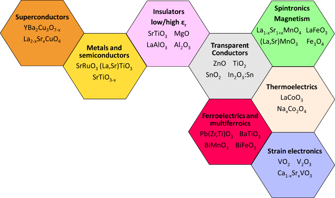
Figure 2: The world of complex oxides
MEMS AND NEMS SYSTEMS WITH OXIDES
Our research activity consists in developing new M/NEMS made by integrating materials different from those used by the MEMS industry, essentially based on silicon, to obtain devices with new functionalities. We develop new manufacturing techniques for M/NEMS and new principles for sensors based on M/NEMS technology. The M/NEMS structures we make also serve as a fundamental research purpose to study the physical and mechanical properties of the materials we deposit in our laboratories. Oxides are among the most interesting materials for the realization of new M/NEMS devices, as it is possible to integrate different oxides into multifunctional crystal heterostructures (a crystal is a periodic arrangement of atoms) that behave as a single mechanical structure. Our devices are made from thin films of crystalline oxides with a thickness of about 100 nm, or 0.0001 millimeters. To do this, we deposit these materials with the pulsed laser ablation technique (see section) and transform them into microstructures using the optical lithography technique and selective chemical etching. One of the main challenges in the development of oxide-based micro- and nanomechanical devices is the precise control of the internal stress of these materials when they have grown in the form of a thin film. The crystalline films grew on a single crystal, also made of oxide, the typical size of a few millimeters that acts as a "substrate". The growth of the new material is influenced by the crystalline structure of the substrate that guides the arrangement of the atoms that form the new film in such a way as to limit stress at the separation interface. This process is called "epitaxial growth" and results in the fact that the distance between atoms (lattice parameters) in a film can be greater or smaller than it would be if the material were made as an isolated single crystal, with the result of being able to produce stressed or compressed films. Suspended structures that are made from thin films can therefore show signs of this stress in a similar way to when you pull or ripple an elastic sheet with your hands. The lattice parameters of the film also depend on the percentage composition of the atoms that make up the lattice. A paradigmatic example of such an effect is (La,Sr)MnO3, a magnetic oxide that shows a ferromagnetic state with a phase diagram (and therefore also with a transition temperature) that depends on the ratio of La to Sr. The La/Sr ratio in (La,Sr)MnO3 also determines the lattice parameters of the compound and therefore the stress that is transmitted to it by the growth substrate. We can grow thin films of La0.7Sr0.3MnO3 or La0.6Sr0.4MnO3 on SrTiO3, a typical substrate for oxide deposition, by varying the deposition parameters. The two films will both exhibit magnetic behavior, but different levels of mechanical stress due to the different atomic radius values of lanthanum and strontium that assign the final size of the crystalline cell.
Pulsed laser ablation (PLD)
Our films are made using the pulsed laser deposition (PLD) technique, a versatile physical vapor deposition technique commonly used for the fabrication of complex oxide thin films. The general principle of PLD is quite simple (Figure 3): a high-power pulsed laser beam (usually an excimer laser) is focused on a target, a sintered product whose percentage composition is usually that of the desired phase, located in a vacuum chamber. The laser beam evaporates ions, neutral atoms, and species from the target into what's called an "ablation plume." In front of the target, about 50 mm away, there is a substrate where the film consisting of the evaporated elements present in the plume begins to grow. Sometimes targets are prepared with a percentage different from the stoichiometry that is to be obtained in the film to compensate for the evaporation of highly volatile elements or their re-emission from the surface of the film itself due to the bombardment of atoms or ions (resputtering). Typical growth rates of films deposited with pulsed laser ablation are in the range of 0.01 nm/laser pulse, approximately 100 nm/hour for a pulse repetition rate of 3 Hz, or 3 laser pulses per second. To obtain good quality crystalline oxide films, however, it is necessary to adjust several growth parameters, such as the temperature of the substrate - which is typically a few hundred degrees Celsius (600 °C - 1000°C) - the pressure of the oxygen in the deposition chamber, usually between 1 mbar and 10-6 mbar, the energy of the laser pulse, which can reach a power of a few MW on a few square millimeters for a period of about 20 nanoseconds (therefore the average power required remains at values manageable by laboratory instrumentation!). The distance between the target and the substrate is also another important parameter to consider when depositing film using PLD.

Figure 3 - A pulsed laser deposition system installed at CNR-SPIN, Genoa unit
Manufacturing processes of suspended structures with oxide films
The fabrication of suspended oxide structures is an essential step in the realization of our devices that include elements capable of moving or oscillating mechanically. It generally starts from a thin film of oxide deposited on a substrate, also made of an oxide, by means of pulsed laser deposition. At this point it is necessary to remove the film in selected areas to obtain the design of the structure to be built and then suspend it. This process takes place in several steps summarized as follows: the film is covered (through the spin-coating technique) with a photosensitive polymer (photoresist) a thickness of a few microns. The desired geometry is transferred to the photoresist film through the optical lithography technique, which allows the photoresist to be removed only in the desired areas with a lateral resolution for our system of about 1 micron. Then we transfer the design created on the photoresist to the thin film by means of a physical or chemical attack (figure 4). The physical attack is performed by the ion milling technique: energetic argon ions bombard the surface of the sample and progressively remove the areas of the oxide film that are not covered by the photoresist. In reality, the photoresist is also slowly removed by argon ions, but its thickness (typically 4 microns) is greater than that of the film in question (about 0.1 microns). During the erosion process, it is also possible to remove part of the substrate, depending on the duration of the process itself. Argon ion erosion is non-selective and removes all materials, each with different specific rates. Oxide films can also be alternatively attacked by chemical methods; in this case each compound has its own selectivity towards specific acids. After the erosion process, we remove the photoresist mask using organic solvents such as acetone, thus leaving its replica imprinted on the oxide film.
As for the suspension or release process, necessary for the construction of the suspended structure, the removal of the regions of the oxide substrate under the film takes place by chemical etching in liquid, using a specific solution capable of removing the substrate without affecting the starting film (figure 4). To do this, we typically explore the different sensitivity of our oxide films to acids of different composition. A typical example is that of manganite ((La,Sr)MnO3) thin films grown on strontium titanate (SrTiO3) substrates: a solution of HF:H2O removes SrTiO3, while it does not affect (La,Sr)MnO3.

Figure 4 - Main processes for the construction of a suspended structure starting from a single film. On the right an image under an optical microscope. The bridge is about 4 microns wide.
The image in Figure 4 shows a suspended microbridge structure made by the processes described above starting from a 100 nm thick magnetic film of (La,Sr)MnO3. The light-coloured area of the bridge is completely suspended. A microbridge of (La,Sr)MnO3 can be entirely suspended by prolonged immersion in HF:H2O solution, as the acid progressively removes the portions of SrTiO3 under the structure of (La,Sr)MnO3, as shown in Figure 5.
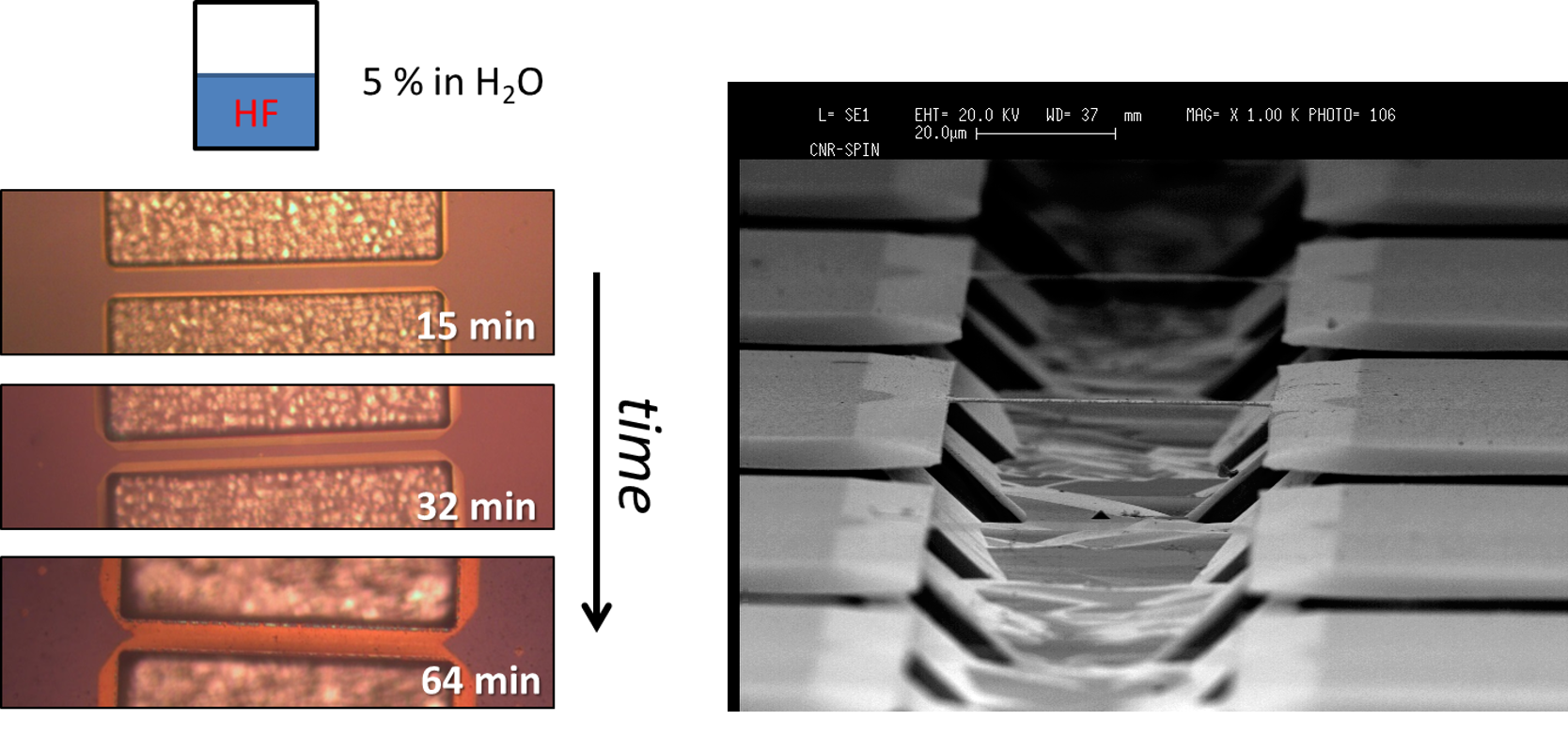
Figure 5 -Preparation of a suspended microbridge by immersion in acid solution. The solution gradually penetrates below the edges of the geometry removing the underlying substrate.
Another fabrication technique employs a sacrificial oxide layer to suspend the structure (support layer) at a precise height above the substrate, which in this case is not affected by the erosion process. For example, an aqueous solution of hydrochloric acid (HCl:H2O) removes (La,Sr)MnO3 but not SrTiO3. Sacrificial layers of (La,Sr)MnO3 can then be employed to fabricate thin-film suspended structures of SrTiO3 by prolonged immersion in HCl, starting from thin-film heterostructures of SrTiO3/(La,Sr)MnO3, Figure 6 (see also Ref. 3). After the chemical attack, the devices are rinsed in water and dried using a special drying method that uses high-pressure liquid CO2 (critical point dryer) to prevent breakage caused by the adhesion forces of conventional drying (e.g. evaporating water or alcohol).
![Figure 6 - Construction of a suspended structure from a sacrificial film [Ref. 3]](/images/Public-engagement/MEMS-construction-FIG6.png "Figure 6 - Construction of a suspended structure from a sacrificial film [Ref. 3]")
Figure 6 - Construction of a suspended structure from a sacrificial film [Ref. 3]
Figure 7 shows some examples of suspended structures made of different oxide films with a thickness of around 100 nanometers.

Figure 7 - Examples of suspended structures with oxide films. The width of the microbridges is about 4 microns. The square island in the center of the trampoline is 20 microns x 20 microns in size.
Mechanical characterization of suspended oxide structures
The fabrication of a suspended oxide structure is the first exciting step in the realization of an M/NEMS device. These tiny structures, suspended a few micrometers from the substrate, are certainly of great impact to the curious eye of a researcher who appreciates their direct vision under the microscope. However, observation under the microscope is only the beginning of a more in-depth and compelling characterization activity, because the suspended structures, when subjected to internal stresses, bend and vibrate at frequencies of the order of hundreds of kHz, well above the audible acoustic range. When we suspend a compressed grown oxide film on its substrate, its final profile can be deformed depending on its internal stress. For example, to release internal stress, a microbridge that is subject to compressive stress bends up or down in proportion to the amount of stress it is subjected to. A paradigmatic example of this was reported by our group for VO2 structures during the structural transition that occurs at about 68°C and involves a change in the internal stress of the whole film.
Figure 8 - Optical microscope image sequence of a VO2 microbridge during warm-up. The VO2 crystal at transition temperature compresses in the vertical direction of the image canceling out the curvature of the edges and expands in the perpendicular direction (horizontal direction) causing the initially tense microbridge to bend. See references in Ref. 2.
The effects of compressive stress on oxide films were also observed in EuTiO3 thin films grown on SrTiO3 substrates. EuTiO3 is an insulating compound with a lattice structure very close to those of SrTiO3. Since it is not affected by hydrofluoric acid (HF), it is possible to fabricate EuTiO3 microbridges and cantilevers on SrTiO3 substrates using a selective etching in HF aqueous solution. A first look at the optical microscope shows microlevers and microbridges slightly bent and the edges suspended between the bases of the microlevers with a "wavy" profile precisely because of compressive stress.
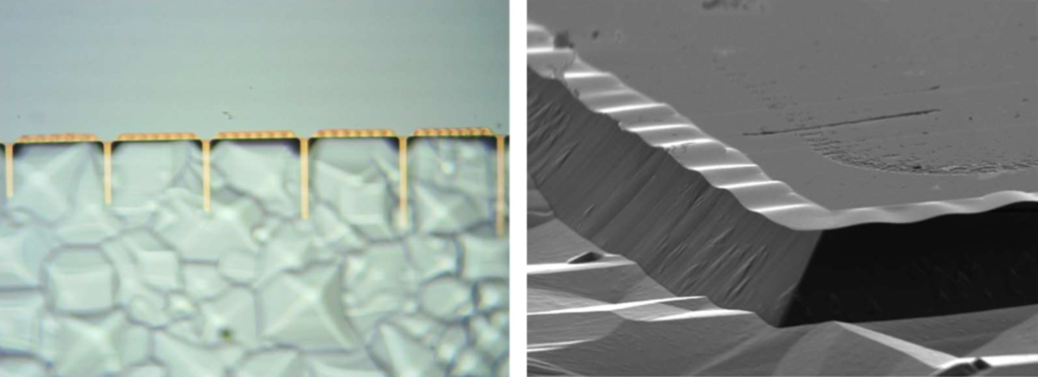
Figure 9 - Suspended structures made of a 100 nanometer thick EuTiO3 thin film. From the curvature of the microlevers and edges, it is clear that the film has grown compressed on the deposition substrate. The microlevers are about 5 micrometers wide.
By analysing microbridges in a more quantitative way by means of an optical profilometer, which allows us to reconstruct the profile of a three-dimensional microscopic object by means of the analysis of reflected light (optical interferometry), we can evaluate the curvature of the microlevers and microbridges fabricated over the entire area of the substrate, calculating the compressive stress value for each of them. We performed this analysis on 140 EuTiO3 microbridges about 100 nm thick and fabricated on a film with side dimensions of 5 x 5 mm2. The calculated average strain of ε = +0.14% ± 0.02% indicates a compression of the crystalline cell in the plane of about 0.55 picometers.
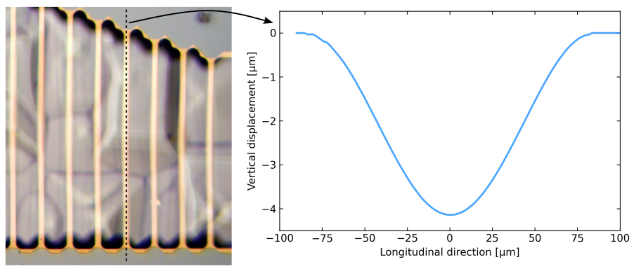
Figure 10 - Curvature of a EuTiO3 microbridge measured with an optical profilometer. Extracted from Ref. 4.
The mechanical measurements on the microlevers of EuTiO3 provide other important information. For example, microlevers can be used to measure how the stress of the film changes along its thickness. Since cantilevers have a free end, the internal tension transmitted by the substrate should relax. However, if the film is not perfectly homogeneous, a small change in tension along its thickness causes a vertical bending of the microstructure.

Figure 11 - Curvature of a EuTiO3 microlever measured using an optical profilometer. The graph on the right is the profile of the lever along the dotted section. Extracted from Ref. 4.
The deformation/curvature relationship of a thin sheet or structure is quite an interesting aspect: a small difference in stress causes a significant change in curvature of the suspended structure and therefore a large vertical displacement of the cantilever (Figure 11). Thin structures can bend long before reaching the maximum allowable stress that leads to their fracture. By measuring the bending profile of EuTiO3 cantilevers, we were able to create a simple model to assess the difference in strain between the bottom and top surfaces of the film. The value found, of about 0.023%, is six times lower than the average strain in the plane. All these static characterization methods allow us to quantify the stress of our structures and correlate it with the structural properties of the starting films.
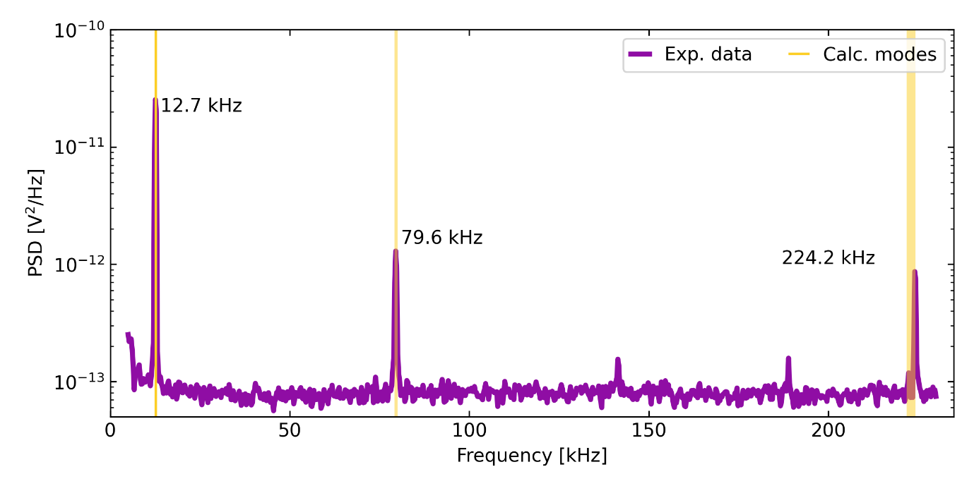
Figure 12 - Mechanical spectrum of a EuTiO3 microlever3. Three main resonances (normal modes) are observed, in accordance with Euler-Bernoulli theory. Extracted from Ref. 4.
Figure 12 shows the "mechanical spectrum" of a EuTiO3 microlever 75 micrometers long and 100 nanometers thick. The structure is set into vibration at each frequency of the interval shown on the x-axis of the graph in the figure, using a piezoelectric element connected to the sample support. Our measuring system uses the principle of optical lever technique via a laser focused on the device. The focused laser light reflects off the surface of the object being measured. The reflected beam changes its position on a detector depending on the inclination of the object itself, allowing to reconstruct, for example, an oscillatory movement. The spectrum observed in figure 12 is therefore the detector signal, which is proportional to the movement of the end of the microlever and is a function of the frequency of periodic mechanical excitation. In the graph in figure 12, each peak corresponds to a mechanical resonance; At the center of this peak, the elongation of the structure for this particular mode of vibration is maximum.
The three peaks observed in figure 12 correspond to the first three modes of flexural vibration of a simple microlever and their value, in terms of frequency, can be adapted to a simple model using the Euler-Bernoulli theory. The resonant frequency of the flexural modes (fn) of our cantilevers is calculated assuming thin and long beams having a width much greater than their thickness (slab approximation) and is described by the following formula:
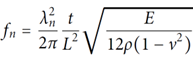
Equation 1: λ n = {1.8751, 4.6941, 7.8548, (2n − 1)π/2 } is a numerical parameter that identifies the normal mode of vibration, t the thickness, L the length, ρ the density of the film, E the Young's modulus, v is the Poisson number.
Note that in Equation 1 there is no stress dependence of the film, but only Young's modulus (E), which can then be directly estimated with a mechanical measurement. Young's modulus gives a quick picture of the elastic behavior of a linear elastic material and is defined as the ratio of the force per unit area to the axial strain of a slab of a given material. The value of Young's modulus that we get in our films is 132 GPa.
In addition to microlevers, we also analysed the vibrations of microbridges made from 100 nm thick films of (La0.7,Sr0.3)MnO3. (La0.7,Sr0.3)MnO3 grows on the SrTiO3 substrate with a tensile-like stress. The microbridges of (La0.7,Sr0.3)MnO3 therefore vibrate like the stressed strings of a guitar and the resonance values of the first bending mode f1 can be described by equation 2.

Equation 2: σ is the stress of the film, L the length of the microbridge, ρ the density of the film.
This "string" limit is valid only for highly stressed microbridges, as in the case represented in figure 13.
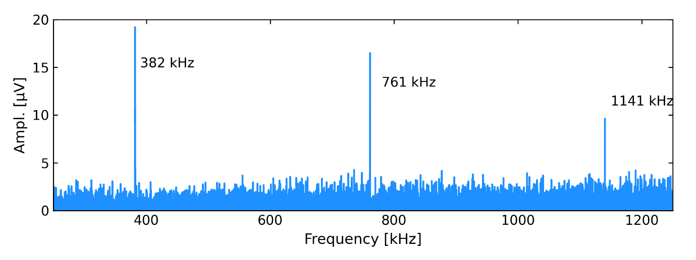
Figure 13 - Mechanical spectrum of a microbridge of (La,Sr)MnO3. Extracted from reference 5.
The measurement of the oscillation frequency of the microbridge therefore provides rapid information on the state of mechanical stress of the film in the area where the device is made. From mechanical spectra such as the one shown in Figure 13, and inverting Equation 2, we can then calculate the local stress σ, which in our case reaches the value of about 260 MPa. Again, it is possible to obtain a spatial map of the stress of the original film and correlate it with other physical measurements to extrapolate useful information, such as the homogeneity of the deposition process.
From dynamic mechanical measurements it is also possible to derive information on the phase transitions of an oxide film. Consider, for example, the case of the ferromagnetic transition of (La0.7,Sr0.3)MnO3, located slightly above the ambient temperature at about 80 °C, which results in a change in the slope of the electrical resistance trend as a function of temperature (figure 14). The magnetic transition also affects the mechanical properties of the film and can therefore also be detected mechanically by measuring the oscillation frequency of the microbridge as a function of temperature. At the transition temperature, the resonant frequency of the microbridge has a change in slope, as shown in figure 14.
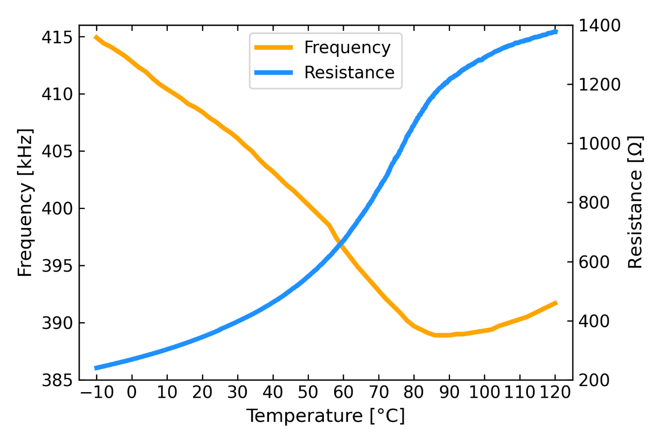
Figure 14 - Electrical resistance and resonant frequency (first flexural mode) as a function of the temperature of a microbridge made with a 100 nm thick film of (La0.7Sr0.3)MnO3 and deposited on a SrTiO3 substrate. Extracted from reference 5.
The marked dependence of the electrical resistance of (La0.7Sr0.3)MnO3 from temperature suggested to use this material to make new thermal detectors operating at room temperature (uncooled bolometers) [Ref. 6]. These devices convert the absorbed heat (e.g. that generated by incident infrared radiation) into a corresponding increase in temperature of their sensitive region and a consequent change in the value of the electrical resistance, which can be quantified by an electronic circuit. A suspended object of (La,Sr)MnO3, such as a microbridge, has advantages in terms of sensitivity as it has a reduced thermal dissipation with the substrate due to the absence of direct contact (except through the bases of the bridge which have a geometrically reduced cross-section) and therefore a greater increase in temperature with the same incident radiation.
Suspended structures can be used as mechanical sensors. A mechanical resonator that vibrates at one of its resonant frequencies is an extremely sensitive object. A perturbation or change in its internal state will modify the value of its mechanical resonance. For example, an added mass will modify the resonance, a localized increase in temperature will modify the internal stress and therefore the resonance itself. External forces, such as electrical or magnetic interactions, can also change the mechanical resonance of a suspended object. Mechanical resonance measurements are very sensitive. It is not uncommon to be able to measure a microstructure that vibrates at 1 MHz and detect a change in its resonance of less than 1 Hz, i.e. measure a physical amount of 1 part in a million! The International Workshop on Nanomechanical Sensing (NMC) focuses on state-of-the-art sensors using these methodologies [Ref. 7].
A fundamental parameter for the development of a resonant sensor is the mechanical quality factor Q, which is a dimensionless parameter defined as the ratio between the energy initially stored in the resonator and the energy lost in an oscillation. Figure 15 is a typical mechanical resonance centered at about 250 kHz and measured on a 500 micrometer long LaAlO3 microbridge like those shown in Figure 4. In the graph of figure 15 the peak has the typical bell shape and is analytically described by the Lorentzian function. The width of the peak at the point where the amplitude of the oscillation is half the maximum value is called the "full width at half height" (FWHM) and is closely related to the Q factor. The higher the Q factor, the less energy is lost during a single oscillation and the narrower the resonance peak will be.
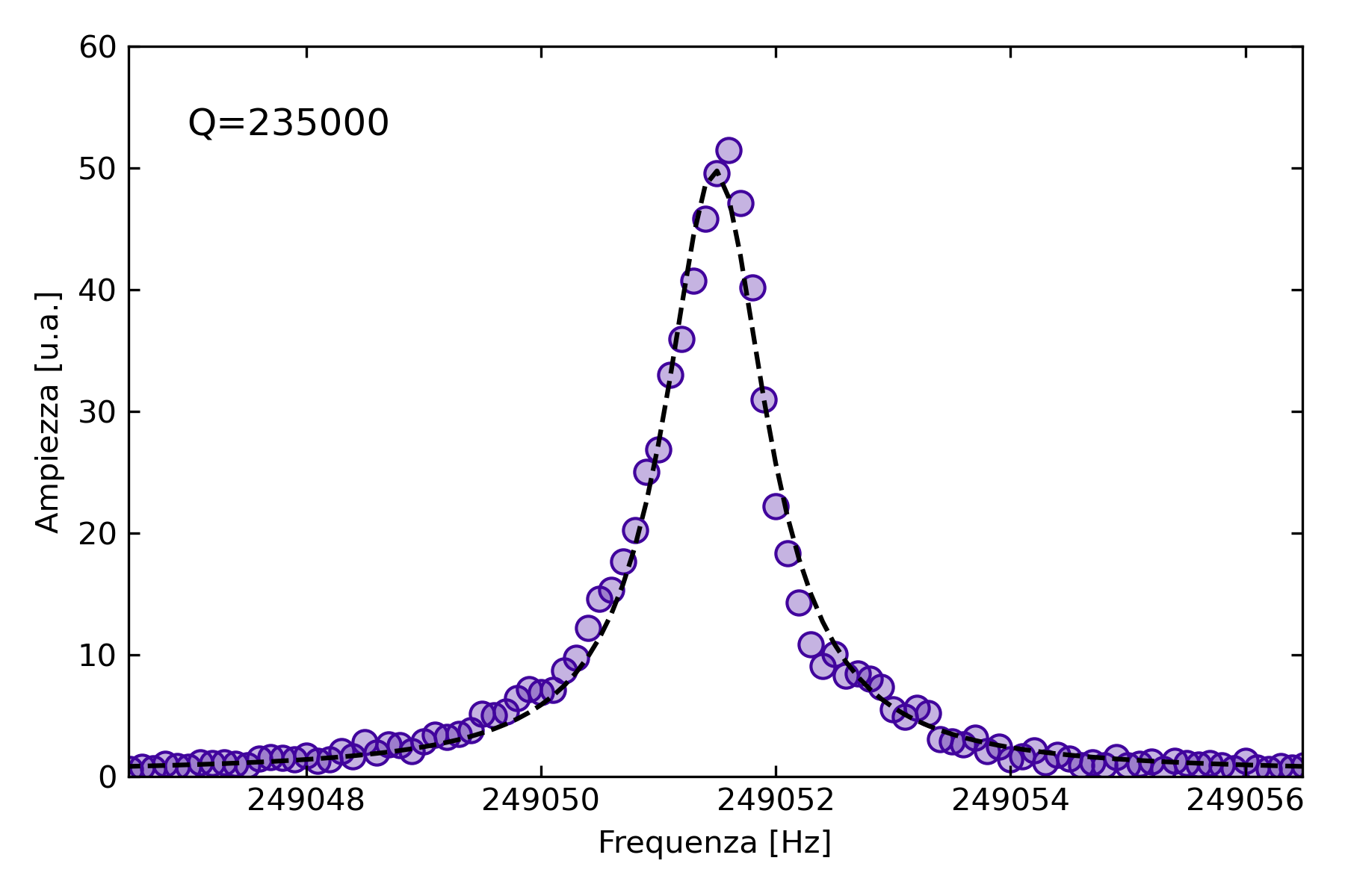
Figure 15 - Resonance peak of a LaAlO3 microbridge 500 μm long and 100 nm thick. The quality factor for this resonator at room temperature and vacuum (10−5 mbar) is about 235000. Extracted from Reference 8.
The energy losses of mechanical resonators have different origins and can be related to air damping, if the resonator operates in ambient conditions, or to the transmission of energy - in the form of vibrations - to the substrate through joints or fixing points. The most dramatic effect is observed when air is extracted around the resonator, especially if the structure resonates with a rather high amplitude as in the case of microlevers and microbridges that also have a low mass (minor effects are observed for mechanical resonances in massive solids). When air is removed, the Q-factor is limited by energy losses within the material and on its surfaces and can easily increase by a factor of a thousand. Q-factors on the order of billions have been detected in silicon nitride-based micromechanical resonators [Ref. 9].
Regardless of its physical origin, resonant detectors need a high Q factor – or a narrow peak resonance curve – to accurately detect the value of the resonance itself and its consequent displacement with the external stimulus. Measuring the Q factor in oxide resonators and understanding how to improve it is therefore of paramount importance for the development of nanomechanical oxide sensors. The observed value has room for improvement as it is probably still limited by dissipation on microbridge surfaces that could be contaminated during the manufacturing process.
The Q factor of microbridges increases with tensile mechanical stress. Our experiments on microbridges with an insulating oxide such as LaAlO3 show a tensile stress in the plane of about 350 MPa and a Q factor that increases linearly with the length of the bridge [Ref. 8]. The measurement of the Q factor allows us to compare the energy dissipation mechanisms of our films and to compare them with other materials generally used in the construction of mechanical devices.
Oxide Integration for Multifunction M/NEMS
As previously reported, many oxides have similar lattice structures and chemical compatibility, so their integration is generally possible. The manufacturing processes we have developed so far and the measurements performed on microresonators made with a single oxide film are just the beginning of an exciting journey aimed at creating mechanical structures composed of different layers with specific functions that contribute to the overall behavior of the resonator. Heterostructures of suspended oxides can therefore be a valid tool for the fabrication of micromechanical devices, both for engineering stress by integrating oxides with different lattice parameters and for the realization of devices in which a specific layer physically or chemically interacts with the external environment.
The integration of different materials requires the development of manufacturing processes that are compatible with all layers and generally involves the use of selective chemical etching procedures. In some cases, however, we have deposited some functional layers directly on top of the suspended structures. As an example, the superconductor YBCO deteriorates easily in contact with acids. To solve this problem, we made microbridges of LaAlO3, an insulating material, on which we then deposited thin films of YBCO by pulsed laser deposition. The YBCO film is therefore the last to be made in the manufacturing process, without interaction with the process chemicals [Ref. 8].
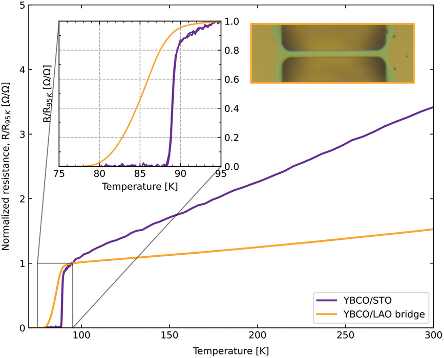
Figure 16 - Superconducting transition (in orange) of a superconductor at high critical temperature (YBCO) deposited over a microbridge of LaAlO3 made by in our laboratories. The purple line refers to the film deposited on a single crystal of SrTiO3. Extracted from Ref. 8.
The deposition of YBCO and other oxides is generally optimized on commercial single crystals of high structural and surface quality, such as SrTiO3 crystals of the typical size of 5x5x0.5 mm3. Hence, the quality of oxide films deposited on suspended structures must be carefully evaluated in a process of optimization of deposition parameters that requires different material analysis techniques.
Conclusions
Oxides offer a wide variety of physical properties and the possibility to be combined together. These characteristics, combined with advanced optomechanical techniques, open exciting prospects for the understanding of these complex materials and for the development of new mechanical sensors and actuators. Building devices that are commercially competitive requires considering the added value of such a rich feature compared to the reliability of the manufacturing process and the cost/performance ratio of current silicon MEMS. Our research also aims to evaluate the potential of oxides to give rise to a new technological line for MEMS and NEMS with these materials. The European OXiNEMS project has been involved in further developing this technology [Ref. 10].
REFERENCES:
1. Mechanics of Microsystems Alberto Corigliano, Raffaele Ardito, Claudia Comi, Attilio Frangi, Aldo Ghisi and Stefano Mariani, John Wiley & Sons Inc (2017) ISBN-10:1119053838
2. Website of the project “Solid State Actuators for Micro/Nanorobotics” www.vo2actuators.spin.cnr.it.
3. All-Oxide Crystalline Microelectromechanical Systems: Bending the Functionalities of Transition-Metal Oxide Thin Films Luca Pellegrino, Michele Biasotti, Emilio Bellingeri, Cristina Bernini, Antonio Sergio Siri, and Daniele Marre Adv. Mater. 2009, 21, 2377–2381
https://doi.org/10.1002/adma.200803360
4. Strain, Young’s modulus, and structural transition of EuTiO3 thin films probed by micro-mechanical methods" by Nicola Manca, Gaia Tarsi, Alexei Kalaboukhov, Francesco Bisio, Federico Caglieris, Floriana Lombardi, Daniele Marré, Luca Pellegrino. APL Mater. 11, 101107 (2023).
https://pubs.aip.org/aip/apm/article/11/10/101107/2915140/Strain-Young-s-modulus-and-structural-transition
5. Stress Analysis and Q-Factor of Free-Standing (La,Sr)MnO3 Oxide Resonators Nicola Manca, Federico Remaggi, Alejandro E. Plaza, Lucia Varbaro, Cristina Bernini, Luca Pellegrino, Daniele Marré ” Small, 18, 2202768 (2022)
https://onlinelibrary.wiley.com/doi/10.1002/smll.202202768
6. Uncooled bolometer response of a low noise La2∕ 3 Sr1∕ 3 MnO3 thin film Laurence Méchin, Jean-Marc Routoure, Bruno Guillet, Fan Yang, Stéphane Flament, Didier Robbes, Radoslav A Chakalov Appl. Phys. Lett. 87, 204103 (2005)
https://doi.org/10.1063/1.2130383 , versione libera https://arxiv.org/pdf/cond-mat/0510176
7. Nanomechanical Sensing workshop series website https://nmc2026.vfairs.com/
8. Integration of High-Tc Superconductors with High Q Factor Oxide Mechanical Resonators N. Manca, A. Kalaboukhov, A. E. Plaza, L. Cichetto Jr., E. Wahlberg, E. Bellingeri, F. Bisio, F. Lombardi, D. Marré, L. Pellegrino. Adv. Funct. Mater. 2403155 (2024).
https://onlinelibrary.wiley.com/doi/full/10.1002/adfm.202403155
9. Strained crystalline nanomechanical resonators with quality factors above 10 billion A. Beccari et al. Nat. Phys. 18, 436–441 (2022).
https://doi.org/10.1038/s41567-021-01498-4
10. Website of the OXiNEMS European project https://www.oxinems.eu/
CREDITS
The contents of the page have been edited by: Luca Pellegrino (This email address is being protected from spambots. You need JavaScript enabled to view it.) and Nicola Manca (This email address is being protected from spambots. You need JavaScript enabled to view it.)
