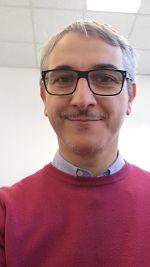
Barra Mario
Senior Researcher

Address
- Complesso di Ingegneria, Scuola Politecnica e delle Scienze di Base, P.le Tecchio 80
- Napoli
- 80125
Contact
- This email address is being protected from spambots. You need JavaScript enabled to view it.
- +390817682548
- +390817682548
- http://orcid.org/0000-0002-1990-0119
Download information as: vCard
Miscellaneous Information
Name: Mario Barra
Birth of date: 30/06/1973
Address CNR-SPIN Uos of Naples and Department of Physics, University Federico II of Naples, Piazzale Tecchio 80, 80125, Naples (Italy)
EDUCATION
2000: Diploma Degree (M.A.) Electronic Engineering, graduating summa cum laude (with full marks), Dep. of Electronic and Telecommunication Engineering, University “Federico II” of Naples;
2004 PHD in Innovative technologies for materials, sensors and imaging, Dep. of Industrial Engineering;
CURRENT EMPLOYMENT
Since Nov 2009: Staff Researcher at the Institute for Superconductors, oxides and other innovative materials and devices (SPIN) of the National Council of Research (CNR), Unity (UoS) of Naples;
PREVIOUS POSITIONS
Oct 2000 - Jan 2001 – Department of Electronic and Telecommunication Engineering, University “Federico II” of Naples, research activity in “Evaluation of the performances of electromagnetic sensors”;
Jan 2001 - Apr 2001 – INFM (National Institute for condensed matter physics), research activity in “Design of superconducting devices for telecommunications”;
May 2001- July 2001 – INFM (National Institute for condensed matter physics), research activity in “Design of superconducting multiplexers and antennas “;
Aug 2001- Dec 2001 – INSTM (National Institute for Materials Science and Technology), research activity in “Design and fabrication of superconducting antennas “;
July 2005 – Nov 2005 – Department of Physics, University “Federico II” of Naples, post-doc research activity in “Modeling of the electrical conduction regimes in organic light emitting diodes”;
June 2004 – May 2005 – Regional Center for New technologies for production activities (CRdC Tecnologie-Scarl - Naples), professional course in “Technology transfer from research centres to industrial world”;
Nov 2005 – Dec 2005 – CNR - INFM (National Institute for condensed matter physics), post-doc research activity in “Characterization of the dielectric properties of insulating films for the fabrication of filed-effect devices based on organic and hybrid semiconductors”;
Feb 2006 – March 2006 – Department of Physics of University of “Federico II” Naples, post-doc research activity in “Characterization of the dielectric properties of insulating films for the fabrication of filed effect devices based on organic and hybrid semiconductors” ;
June 2006 – Jan 2007 – Regional Center for New technologies for production activities (CRdC Tecnologie-Scarl -Naples), professional course in “ Product and process innovators in Small and Medium Enterprises”;
July 2007 – Nov 2009 – Department of Physics of University of Naples Federico II, post-doc research activity in “Fabrication and characterization of hybrid organic-inorganic devices”
SCIENTIFIC VISITS AND STAGES
Mar 2003 - Sept 2003 – Scientific visit at UPC (Università Politecnica de Catalunya), Barcelona (Spain), working in the group of Prof. Joan O’ Callaghan on “Fractal resonators for superconducting planar filters”;
Mar 2005 - Apr 2005 – Stage at ST Microelectronics (Naples) with a project on “Fabricaton and electrical testing for Organic Light Emitting Diode”;
Jan 2007 - June 2007 – Scientific visit at Institute for Nanostructured Materials (ISMN) of CNR, Unity of Bologna (Italy) of CNR, working in the group of Dr. Alek Dediu “Deposition techniques of organic thin films”;
May 2011 – Scientific visit at the Department of Condensed Matter Physics, University of Geneva (Switzerland), working in the group Porf. A. Morpurgo on “Ionic liquid techniques applied to Organic Transistors”;
RESEARCH ACTIVITY
Since the beginning, the activity research of Mario Barra has been devoted to the study of the electromagnetic properties of innovative materials and to the development of related devices suitable to be utilized in different application fields. During the years 2000-2004, the activities were mainly focused on the design, fabrication and experimental testing of planar microwave devices based on superconducting films. The development of miniaturized superconducting planar filters for mobile communications was the main subject of study. Starting from 2005, the scientific work has been basically committed to the investigation of the charge transport phenomena in organic functional materials and on the fabrication and electrical characterization of electronic devices, such as Light Emitting Diodes, solar cells, sensors, and transistors based on these materials. For the characterization of materials and devices, a wide series of techniques operating both in DC and AC regimes, up to the microwave range, has been applied. At present, the main scientific interests are:
- Growth and morphological characterization of organic films;
- Charge transport at micro and nano-scale in high-performance organic semiconductors;
- Charge-transfer and doping effects in organic and hybrid materials;
- Impedance spectroscopy techniques for electronic and bio-electronic applications;
- Ionic/electronic transduction effects in organic field-effect and electrochemical transistors;
- New functional electronic systems combining 2D materials and organic molecules.
TEACHING ACTIVITY
Co-supervisor of about 25 master thesis (I and II level) in Electronic, Biomedical and Chemical Engineering.

