Here you can find a brief journey to discover what the transistors are, why and when they were invented and which are now the transistor families investigated by SPIN researchers.
The content of this page was particularly conceived for high school students.
For further insights, you can refer to the videos and documents mentioned in the references section.
- Electronics: the origins
- 1947: the first transistor
- 1960: the birth of MOSFET
- Thin-film electronics
- Organic semiconductors
- Organic transistors and ongoing research activities
- References
Electronics: the origins
The ability to create increasingly miniaturized electronic circuits with higher operating speeds is one of the cornerstones of the information society we live in. In almost all cases, such systems are based on the integration of a vast number of elementary devices known as transistors. In a modern silicon chip, several billion of these transistors can be found within just a few square centimetres, and when properly interconnected, they enable a wide range of operational functions. The history of modern electronics dates back to the early 20th century with the invention of the first “thermionic valves” in diode and triode configurations, developed, respectively, by John Ambrose Fleming (1904) and Lee De Forest (1907).
In both cases, within glass bulbs containing rarefied gases, the ability to extract electronic charges from heated metal filaments (cathodes) was exploited by applying an electric field via a second electrode (anode). In the device developed by De Forest (Fig. 1a), also known as the Audion, a third electrode (the grid), placed between the anode and cathode, allowed modulation of the current flowing between them. This made it possible to amplify the input signal (applied to the grid), which quickly found its first application in the telephone systems that were spreading across the United States in the early decades of the 1900s. The use of these devices, and their subsequent refinement, led to the development of the first real electronic systems utilized both in telecommunications, from television to radar systems, and in the first large computers, already employed by the end of World War II for decrypting coded messages. (1)
Despite their widespread use, “thermionic valves” had some fundamental drawbacks: they were bulky, making further miniaturization impractical; they required high electrical power to operate (often many watts); and they were structurally fragile. In this context, throughout the first half of the 20th century, significant efforts were made to develop alternative electronic devices that could offer the same amplification properties without the aforementioned disadvantages.
The main focus was placed on the new class of semiconductors, whose electrical behaviour was correctly understood during that period thanks to advances in modern solid-state physics, founded on the principles of the then-emerging quantum mechanics. In the first half of the 20th century, much attention was devoted to fabricating various devices with rectifying response (i.e., current could pass in only one voltage polarity) for use in radio signal receiving systems.
As interest shifted toward microwave radar applications, efforts were concentrated on so-called "cat-whisker" rectifiers, which involved forming metal contacts on semiconductor substrates. Since the functionality of these systems depended critically on the quality of the semiconductors used, especially under the wartime pressure of the early 1940s, various processes were developed to produce silicon or germanium samples with levels of purity never before achieved.
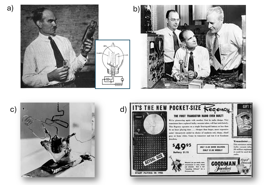
FIG.1
1947: the first transistor
This was the context in which, immediately after the end of the World War II, research into replacements for bulky thermionic valves regained momentum. Among the first to move in this direction were the Bell Labs, the research division of AT&T, the company that had extended the telephone system across the United States since the early 20th century. To this end, as early as the mid-1930s, Bell Labs had established highly interdisciplinary research teams. It was from one of these teams, comprising William Shockley, Walter Brattain, and John Bardeen (Fig. 1b), that the first experimental demonstration of a new device, later named the “transistor,” emerged. The name was proposed by John R. Pierce, also a researcher at Bell Labs.
After initially exploring the possibility of influencing electrical conduction on a germanium surface through the application of a strong external electric field, a theoretically plausible phenomenon though not observed experimentally due to the dominant presence of surface defects in the semiconductor samples available at the time, the first “point-contact” transistor (Fig. 1c) came to light just a few days before Christmas in 1947. This achievement was largely due to the theoretical insights of Bardeen and the experimental inventiveness of Brattain. In this device, two gold contacts, spaced less than a millimetre apart, were pressed onto a germanium wafer. (2, 3)
The current between the two contacts could be modulated by applying a signal to a third electrode, which, being located on the opposite side of the semiconductor wafer, was called the “base”. The operating principle of the first transistor is not easy to describe, and some details remain elusive even to specialists (see reference 4 for further insight). The key element, however, was related to the presence in the semiconductor of one region (the base) rich in electrons (thus called N-type), and another (the upper region where the gold electrodes were placed) deficient in electrons, and therefore rich in vacant sites (holes) that could be occupied by electrons (this region was called P-type). In practice, the device’s ability to amplify an input signal was made possible by the interaction between the current carried by the flow of electrons and a second current due to the movement of holes. These same principles were later further developed by Shockley, who, in the following years up to 1951, introduced the concept of the bipolar junction transistor (BJT), in which P-type and N-type semiconductor regions were arranged in a more functional manner.
The term “bipolar” specifically refers to the presence of two types of charge carriers in the device. The amplification properties of the early versions of transistors led to their immediate adoption for commercial use (5, 6), as demonstrated by the release of the first transistor radio, the Regency TR-1, already on the market in 1954 (Fig. 1d).
1960: the birth of MOSFET
During the 1950s, innovations made possible by the optimization of materials and fabrication processes, alongside a deeper understanding of the physical behaviour of semiconductors, led to the development of new types of transistors. This culminated in 1960 with the first demonstration, by Mohamed Atalla and Dawon Kahng, again at Bell Labs, of the Metal-Oxide Semiconductor Field-Effect Transistor (MOSFET), which remains by far the most widely used type of transistor in modern digital electronic circuits, where information is encoded as combinations of binary signals.
A MOSFET (Fig. 2a shows a possible layout with the indication of P-type and N-type regions) is a unipolar device (namely, only electrons or only holes flow through the main channel) where the current between the drain and source electrodes is modulated by applying a voltage signal (VG) to the gate electrode, which is separated from the main channel by a thin dielectric (insulating) barrier. In this configuration, silicon has definitively established itself as the most versatile material, thanks also to the superior technological properties of its oxide (SiO2), which is used to form the insulating layer. In a MOSFET, the key phenomenon is known as population inversion: when induced by the gate signal, it creates direct electrical communication between the source and drain electrodes (Fig. 2b). In the absence of such a signal (Fig. 2a), and regardless of the voltage applied between drain and source, at least one of the junctions at the drain/substrate or source/substrate interface is “reverse-biased”, allowing only weak currents to pass (7).
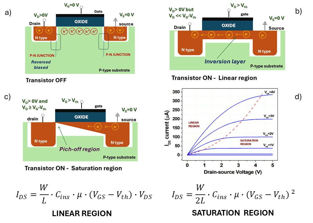
FIG.2
When VG exceeds a certain threshold voltage (Vth), population inversion occurs, and the current between drain and source (IDS) increases significantly, depending on both the drain-to-source voltage (VDS) and the gate voltage VG. Figure 2d shows a typical example of MOSFET output curves, illustrating the two main operating regions: the linear region (Fig. 2b) and the saturation region (Fig. 2c). These regions are characterized by different charge distributions in the channel and specific dependencies of IDS on VGS and VDS, as described by the equations at the bottom of Fig. 2. In those equations, the mobility (µ) of the charge carriers (electrons or holes) is the key electrical parameter defining the material’s performance.
The invention of the MOSFET essentially laid the foundation for the birth of modern microelectronics, which truly took off once technological processes were developed that allowed for the “integration” of multiple devices on the same semiconductor substrate. To this end, the contributions of numerous scientists were crucial, especially in the continuous optimization of photolithographic techniques first introduced in 1959 by Jay W. Lathrop. Today, the use of extreme ultraviolet lithography (8) represents one of the most complex technological processes ever developed by humankind and, together with the introduction of new three-dimensional (9) transistor architectures, lies at the heart of the latest generation of chips.
Thin-film electronics
Alongside the development of modern micro/nanoelectronics based on crystalline silicon, research has also continued over the decades into new semiconductors suitable for the development of devices used in other application areas. In this regard, it is important to mention the emergence of thin-film transistors (TFTs), which are based on the use of semiconductors that can be deposited as layers just tens or hundreds of nanometers (10⁻⁹ m) thick on insulating substrates (10). The first experimental demonstrations of TFTs were achieved between the late 1950s and early 1960s, using germanium films for the active channel and germanium oxide as the dielectric barrier. During the 1960s and 1970s, further experiments followed, highlighting the semiconducting performance of alternative materials such as cadmium selenide (CdSe).
The real breakthrough in the field came in 1979 with the development of TFTs based on amorphous silicon (which completely lacks the structural order of the crystalline silicon used in MOSFETs and BJTs). This advancement opened the door to the definitive application of these devices in the emerging sector of liquid crystal displays (LCDs), which were commercialized throughout the 1980s. From the 1990s onward, the development of thin-film electronics further drove research aimed at identifying additional semiconducting compounds capable of offering the best possible trade-off between electrical performance (such as charge carrier mobility) and reduced fabrication costs. This was pursued through the use of increasingly lower processing temperatures to expand the range of substrates compatible with thin-film deposition.
As a result, new classes of materials have emerged, including transition metal oxides (many of today’s modern LED screens are driven by transistors based on a zinc oxide variant called IGZO), organic semiconductors, carbon nanotubes, hybrid organic-inorganic compounds, and two-dimensional (2D) materials. Some of these materials, which remain the subject of intense research activity, are also of interest for the development of electronics that are fully transparent to visible light.
Organic semiconductors
Within the research activities of the SPIN Institute, organic semiconductors, compounds based on carbon and a few other atomic species such as hydrogen, nitrogen, oxygen, and sulfur, represent a significant field of interest. The structure of these compounds (Fig.3a), in the form of molecules or polymers, is characterized by fused aromatic rings with alternating single and double bonds between carbon atoms (conjugation).
Double bonds (Fig. 3b), in particular, are characterized by the presence of so-called π-electrons, which occupy a distinctive double-lobed orbital. In aromatic rings, these electrons are more delocalized compared to the original atomic structures, making them more "mobile" when subjected to an external electric field. This scenario is radically different from what occurs in conventional plastics (also primarily carbon-based), where the presence of only σ-bonds (Fig. 3c) gives the material a predominantly insulating character from an electrical standpoint. In general, organic semiconductors can be processed at temperatures below 200 °C and some of them are also soluble in suitable solvents. This makes possible their deposition as thin films even on flexible substrates.

FIG.3
Furthermore, the ability to chemically modify their molecular structure has enabled the evaluation and optimization of many organic materials by improving their self-assembling properties. This term refers to processes in which a system of initially disordered components organizes itself into a spatially ordered structure due to specific local interactions among the components. Indeed, it is the spatial arrangement of molecules in the resulting solid-state structures (whether thin films or crystals) that primarily determines how effectively electronic charges can move under the influence of an electric field, thereby producing different values of mobility. Another notable feature of organic compounds, which is basically related to their chemical composition and the mechanical properties typical of soft materials, is their often high degree of biocompatibility. This makes them promising candidates for use in electronic interfaces capable of operating in contact with living matter or, more broadly, in biological environments.
The history of organic semiconductors is also somewhat longer than one might expect, with some studies already highlighting their electrical properties back in the 1940s (11). However, one of the major breakthroughs in the field, also recognized by the 2000 Nobel Prize in Chemistry (12), was the 1977 demonstration by Alan G. MacDiarmid, Alan J. Heeger, and Hideki Shirakawa that the electrical conductivity of a polymer (specifically, polyacetylene) could be significantly increased by exposure to halogen vapours (Br, Cl, I), reaching values (~10⁵ S/cm) comparable to those of metals.
Organic transistors and ongoing research activities
It wasn't until 1986, however, that the first demonstration of an organic transistor, based on a film made from an undoped polythiophene compound, was achieved by researchers at Mitsubishi Electric Corporation (13).
In most cases, the structure of an organic transistor is like the one shown in Fig. 4a, with a semiconducting film in contact with the source and drain electrodes and separated from the gate electrode by a thin dielectric barrier (ranging from several hundred to just a few tens of nanometers). As in other field-effect transistors, the current flowing through the active channel can be modulated by a voltage applied to the gate, which primarily induces an “accumulation” of charge at the interface with the dielectric barrier. Although the physical mechanism differs from that of MOSFETs (population inversion vs. charge accumulation), the electrical behaviour of an organic transistor is generally described, with reasonable approximation, using the same equations (Fig. 2). To this day, research in this highly interdisciplinary field continues to focus on identifying new compounds that, thanks to improved self-assembling properties, can form films with better electrical properties (namely, increased charge carrier mobility).
Over the past 40 years or so, the mobility values in organic transistors have improved dramatically, from around 10⁻⁵ cm²/V·s to values exceeding 10 cm²/V·s which now surpass the performance of amorphous silicon. Research efforts are also focused on understanding and mitigating the physical phenomena that lead to non-ideal behaviour in organic transistors. Among these, it is to be mentioned the mechanisms that cause charge trapping, which lead to a progressive reduction in current over time during operation (known as bias stress). Another major area of investigation concerns the mechanisms that hinder charge injection or extraction via the source and drain electrodes (typically made of metal) in contact with the organic channel. These issues give rise to so-called contact resistances at the metal–organic interfaces, which in practice degrade the electrical response, particularly as the channel length is reduced to values below a few tens of microns.
In addition to these more fundamental research directions, current efforts are also aimed at demonstrating the practical usability of organic transistors in various application areas, particularly in the development of innovative sensors. At the SPIN Institute, ongoing work includes the fabrication of organic transistors on flexible substrates (Fig. 4b) for the detection of ionizing radiation and/or optical signals. The goal in this context is to develop flexible devices, capable of conforming to the shape of the human body, for real-time use as dosimeters during therapies involving the irradiation of human tissue with proton beams. Another possible application is the development of devices sensitive to visible light that can be used in broadband communication systems. Here, the wide variety of organic compounds can be effectively leveraged, as their sensitivity to different wavelengths (and thus colours) of light can be tuned by altering the size of their molecular structure.
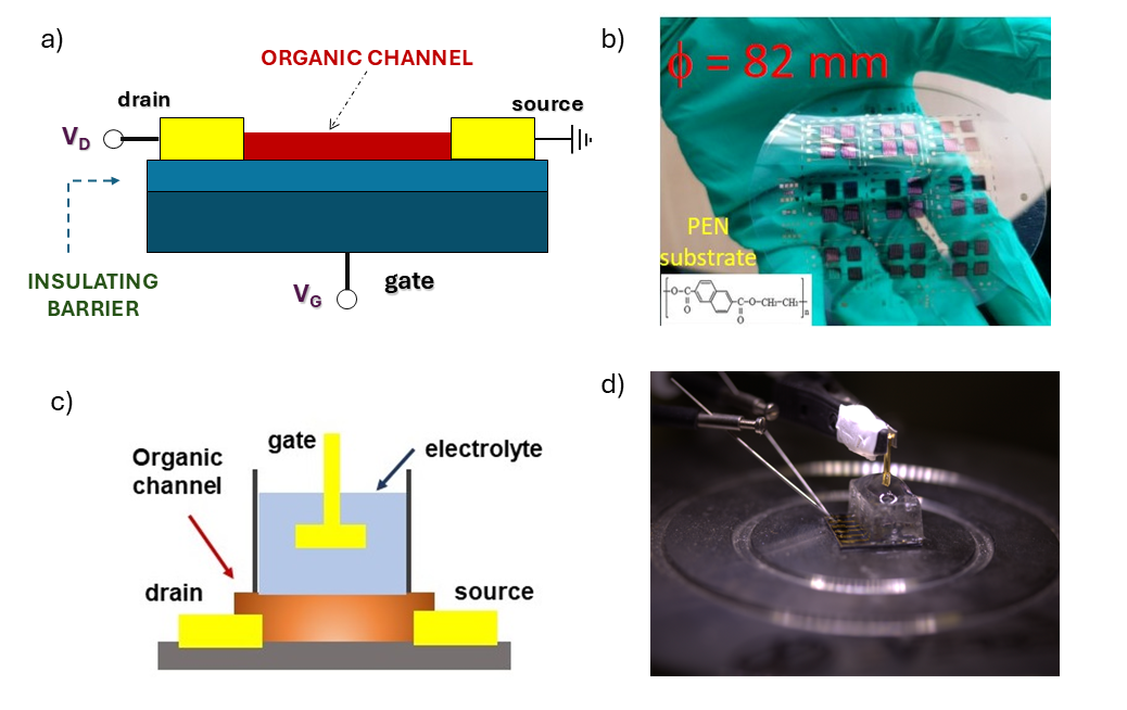
FIG.4
Different types of organic transistors can also operate in liquid environments, with voltages below 1 V, allowing the detection of specific biologically derived substances (e.g., biomarkers related to certain diseases). In this case (Fig. 4c, d), the organic channel is immersed in an electrolyte, which also contains an additional conductive element (which can be integrated on the same substrate as the channel) that serves as the gate electrode. The signal applied to this contact modulates the current flowing through the organic material by leveraging the movement of ions present in the electrolyte, thus enabling direct transduction of ionic signals into electronic ones. In this context, a distinction is made between organic materials that are impermeable to ions and those that are porous to the ionic flow. In the latter case, the transistors are referred to as "electrochemical" transistors. Through specific chemical-physical processes, the gate electrode can be functionalized with biological elements (e.g., antibodies) capable of specifically recognizing a target substance in the electrolyte.
Ultimately, this feature allows the transistor's response to be specific to a particular biological "target," whose concentration is correlated with the variation of one or more electrical parameters of the device (e.g., carrier mobility, threshold voltage). The goal of this approach is to develop biosensors that are low-cost, compact, lightweight, yet capable of delivering highly sensitive and selective responses. These characteristics are critical to create high-performance diagnostic systems that minimize the occurrence of false negatives (failure to detect a substance even when present) and false positives (false detection of a substance when absent).
At the end of the following section, you can access to a few scientific articles published in recent years by SPIN researchers on the topics discussed here.
- COLOSSUS - Computer History Museum: https://www.youtube.com/watch?v=7cDeG3hyraA
- AT&T Archives: Genesis of the Transistor: https://www.youtube.com/watch?v=WiQvGRjrLnU
- Storia dei primi transistor: https://www.youtube.com/watch?v=Pzy_KOBddRA&t=1222s
- How the First Transistor Worked: https://spectrum.ieee.org/transistor-history
https://www.youtube.com/watch?v=MFN2p8izhss - The Transistor: a 1953 documentary, anticipating its coming impact on technology: https://www.youtube.com/watch?v=V9xUQWo4vN0
- Transistor Full Documentary: https://www.youtube.com/watch?v=U4XknGqr3Bo
- MOSFET Transistor Basics & Working Principle: https://www.youtube.com/watch?v=p34w6ISouZY
- The Extreme Engineering of ASML’s EUV Light Source: https://www.youtube.com/watch?v=5Ge2RcvDlgw&t=214s
- The 3-D Transistor Transition: https://www.youtube.com/watch?v=i3dDslo9ibw
- Thin Film Transistor Technology—Past, Present, and Future: https://iopscience.iop.org/article/10.1149/2.F06131if
- D.D. ELEY ,Phthalocyanines as Semiconductors Nature vol. 162, page 819 (1948): https://www.nature.com/articles/162819a0
- The Nobel Prize in Chemistry 2000: https://www.nobelprize.org/prizes/chemistry/2000/summary/
https://www.youtube.com/watch?v=wKICpWFMOvI - First demonstration of a transistor based on a polymer channel: Tsumura; H. Koezuka; T. Ando, Macromolecular electronic device: Field‐effect transistor with a polythiophene thin film, Appl. Phys. Lett. 49 (18). 3 November 1986
https://pubs.aip.org/aip/apl/article/49/18/1210/51910/Macromolecular-electronic-device-Field-effect
Other videos and stories are available on the website and youtube channel of the Computer History Museum (USA)
Open access papers
- Perylene-Diimide Molecules with Cyano Functionalization for Electron-Transporting Transistors, Electronics 2019, 8(2), 249;
https://www.mdpi.com/2079-9292/8/2/249 - Flexible fully organic indirect detector for megaelectronvolts proton beams, npj Flexible Electronics volume 7, Article number: 5 (2023),
https://www.nature.com/articles/s41528-022-00229-w - Organic Electrochemical Transistor Immuno-Sensors for Spike Protein Early Detection, Biosensors 2023, 13(7), 739;
https://www.mdpi.com/2079-6374/13/7/739
CREDITS
Mario Barra (This email address is being protected from spambots. You need JavaScript enabled to view it.), Fabio Chiarella (This email address is being protected from spambots. You need JavaScript enabled to view it.), Ettore Sarnelli (This email address is being protected from spambots. You need JavaScript enabled to view it.)